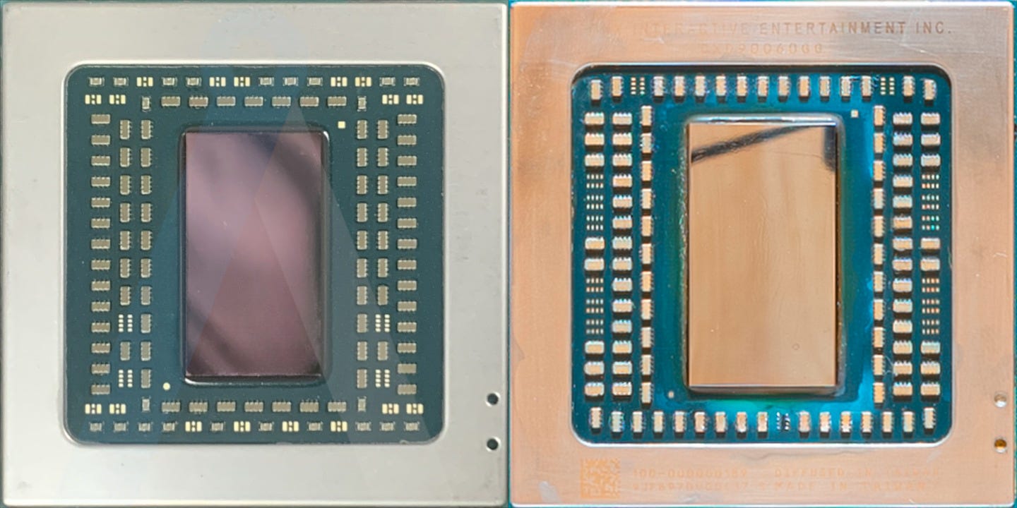
In the last month, Sony has begun the rollout of their latest revision of the PlayStation 5, model CFI-1202. There has already been a teardown showing the model’s redesigned board and cooling that is smaller and lighter. Power consumption is also reduced while giving similar performance. To accomplish this, AMD’s Semi-Custom design teams have ported the PS5 silicon to TSMC N6, codename Oberon Plus. Angstronomics reveals exclusive images of the new, smaller die, and we discuss the how and the why behind this update.
How Die Shrinks Work
These console refreshes are the modern-day equivalent of what used to happen decades ago in the microprocessor industry, where existing designs would be ported to a new, more efficient process node with minimal rework. For this example, TSMC ensures that their 6nm EUV process is Design Rule Compatible with their N7 DUV process, meaning that customers can reuse existing designs made for N7 to use on N6, with a simple conversion process that does not alter the underlying high-level synthesis.
Along with an 18.8% increase in logic transistor density thanks to CPODE (which you can learn about in our article here), N6 also lowers power consumption for a given performance level vs N7. This is what enables the reduced wall power of the latest PS5 revision, with less requirement for heat rejection and hence a smaller, lighter cooler. As TSMC completes its transition to increase EUV adoption and move most products to N6 from N7, we get updates like Oberon Plus. While most fabless companies would just design a new product on N6, game consoles demand absolute low-level platform hardware and software compatibility. This is why we see the exact same design being ported with zero configuration changes, including keeping with the reduced Floating Point Unit in the Zen 2 CPU cores (which we will also see in Ryzen 7020 Series ‘Mendocino’).
Oberon Plus
With an exclusive side-by-side comparison showing 6nm Oberon Plus next to 7nm Oberon, we can see what has physically changed in the 2 years between them. Die size has gone from ~300 mm² to below 260 mm², a shrink of close to 15%. What this means in the end is that each wafer processed can produce near 20% more chips for a similar cost.
It’s All About the Money Margins
The game console business works on selling hardware cheap and generating revenue in game sales. As such, it is paramount to minimize production costs to generate meaningful profit margins. With the aforementioned smaller die and lighter cooler enabled by lower power consumption, we estimate that each new PS5 going forward costs Sony around 12% less to make overall, which helps to recoup program development costs sooner than if no die shrink took place.
As the PS5 is the most produced out of the 3 current generation consoles (PS5/XSX/XSS), it sees the biggest benefit moving to N6 first. Going forward, only Oberon Plus will be produced, and 7nm Oberon production stopped. And while one can make near 50% more PS5 chips per wafer than Xbox Series X chips, the latter will also get its 6nm update of Arden in the future.


This makes sense, whatever Sony has to do to get away from Liquid Metal. Should save them a pretty penny and save them from headaches in the long run as well.
thaaaaanks man