Computex: Beyond the Coverage
What they didn't tell you.
In this second article on Angstronomics, we go beyond the Press Deck and discuss the interesting observations we picked up on during the week of Computex Taipei 2022 from AMD and NVIDIA. We will also add our own flavor into the mix with exclusive information we can reveal about some products. Enjoy!
But first:
A huge thank you to all those who have read and subscribed to our fledgling publication! In less than a week, with just one article, we have amassed over 10,000 unique visitors and received over 100 subscriptions, far exceeding our humble expectations!
A big tip of the hat to the Hacker News community, who were quick to share and discuss our article! While we do try to promote our articles on Twitter (which readers should follow for timely updates and insights), the HN post gave us a huge boost. Thank you!
We have big plans for Angstronomics moving forward, including process deep-dives, past and future events, and more exclusive info! Read on to the end to see what is in the works!
For our new folks, do Share and Subscribe to receive our articles right in your inbox!
- SkyJuice, Founder of Angstronomics
Socket AM5 Motherboards
As expected, Computex Taipei 2022 played host to the announcement of several Socket AM5 motherboards for AMD’s upcoming Ryzen 7000 Series Desktop Processors. This makes sense as these board makers are based in Taiwan and have the majority of their board manufacturing capability on the island. A wide spectrum of boards have been revealed, with many different configurations of expansion slots and ports on offer, indicating the vast optionality built-in to the I/O system of the CPU and the accompanying 600-series chipsets, which we detailed here.
From Thunderbolt and USB4 to 10GbE and even up to four PCIe 5.0 M.2 slots for storage, board makers are free to differentiate their designs through different PCIe lane bifurcation and ports enabled. Furthermore, AM5 600-series board prices seem to indicate more features for a similar or lower list price than the previous generation X570 boards, possibly contributed by the lower cost of the ASMedia chipsets compared to reusing the IO die for X570’s Bixby chipset.
AMD’s Computex Keynote presentation promoted 24 lanes of PCIe 5.0. The IO Die on the AM5 Processor does have the PCIe controllers and Physical Layer (PHY) for 28 lanes of PCIe 5.0 throughput. However, attached devices such as USB4 controllers and the ASMedia-made 600-series chipsets can only support up to PCIe 4.0 linkrate. As 4 lanes are occupied by the chipset downlink, this leaves 24 PCIe 5.0 lanes for the board makers to utilize.
From our block diagram, you can also know that ‘Up to 14 SuperSpeed USB’ really means an X670 daisy-chained solution, with four 10Gbps USB from the CPU Combo ports, and one 20Gbps USB and four 10Gbps USB from each of the two chipsets. That sums to 14 SuperSpeed USB ports, of which 2 are 20Gbps and 10 are 10Gbps. WiFi 6E support is through discrete PCIe M.2 Key-E cards from vendors such as MediaTek and Qualcomm. Finally, as we indicated earlier, the integrated graphics of the processor also supports up to 4 Displays, either HDMI 2.1 or DP 2.0 UHBR10.
The phrase ‘Up to’ is necessary here as from our article, 3 display outs are part of USB Type-C Combo ports. Mainboard designers can place a Type-C port that can switch between either 10Gbps USB or DisplayPort Alt-mode. If they choose to connect the combo port to a 10Gbps USB Type-A, then there will be one less display out option. Alternatively, they could assign it to a dedicated HDMI 2.1 port, in which case the combo port’s USB function drops to USB 2.0, removing a SuperSpeed USB option.
We did not indicate the die size of the ASMedia chipsets in our previous article, but thanks to a livestream by MSI, we can determine the die size to be ~40 mm². This is far smaller than the 125 mm² of the previous X570 chipset, which had many disabled regions but more I/O capability. Lower area reduces cost of fabrication.
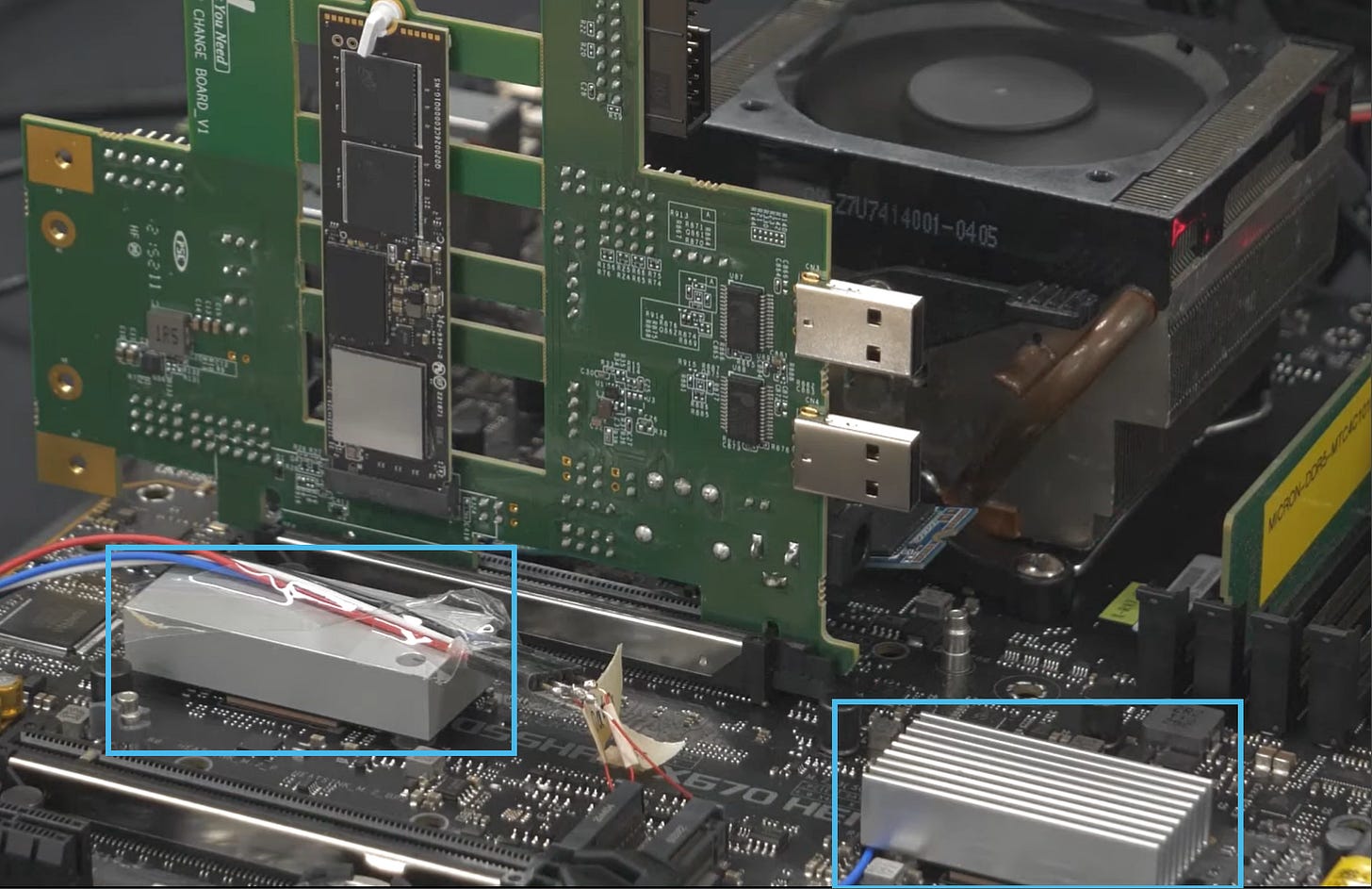
Notice the chipset arrangement of the MSI X670 board, which groups the pair at the traditional bottom-right region of the motherboard. This contrasts with the ASUS X670 board, revealed in Phison’s E26 PCIe 5.0 SSD controller demo, which places the chipsets further apart in an East / West orientation. We explain why this is beneficial in our previous article.
Raphael Revealed
Shown on stage and in a Tweet, the chiplet configuration of AMD’s Ryzen 7000 series, codename Raphael, was revealed by AMD CEO Dr. Lisa Su, showing the individual dies and capacitor arrangement. The sample shown has been taken off the production line before the lidding process, as shipping units have an Integrated Heat Spreader (IHS) covering the dies. With this, we can do an estimate of the die sizes.
Ryzen 7000 series Desktop ‘Raphael‘ Processors:
AM5 socket 1718-position Organic Flip Chip Land Grid Array: 40 x 40 mm
IOD (Input Output Die) on TSMC N6: ~ 120 mm²
CCD (Core Compute Die) on TSMC N5: ~ 72.5 mm²
As a side note, we notice that the CEO held the processor upside down. The corner triangular Gold indicator is always oriented in the top-left corner when installed on a standard Desktop motherboard.
Going for Gold
The most striking observation of Raphael’s dies are the Gold colour of the CCDs, while the IOD remains the usual grey of Silicon. This Gold colour comes from the silicon Backside Metallization (BSM) that contains a layer of Gold a few hundred Angstroms thick. The Gold layer is beneficial for silicon that is going to be soldered and lidded, as it prevents oxidation of the silicon and formation of tiny gas voids during heating, which is required to melt the Indium-based solder Thermal Interface Material (TIM) during the lidding process where the IHS is also attached.
Solder is used as the thermal link from the silicon dies to the IHS as it has low thermal impedance and can be melted and reflowed to fill any air gaps and rough surface finishes. The Gold layer also provides a better wetting surface for the melted solder to adhere to and flow across the silicon. While we are starting to see this Gold BSM process applied to more products such as Intel’s Sapphire Rapids and Ponte Vecchio Processors, this is not required for processors designed for direct die cooling like NVIDIA’s Hopper H100 GPU as there is no need to attach solder.
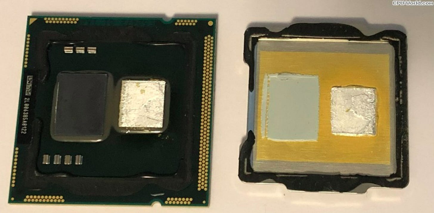
Likewise, a Gold coating is applied on the underside of the IHS for much the same reasons, shown below with Intel’s Clarkdale as a clear example.
If the CCDs have this Gold coating, why doesn’t the IOD also have it? It could be due to cost reasons. The BSM step is applied to whole wafers prior to dicing, so clearly the step was omitted on the IOD wafers, perhaps due to the low heat density of the IOD not requiring this additional, cost-adding process.
Packaging Engineer Tom Wassick indicates that all dies under solder TIM have this BSM process layer, so perhaps AMD may be mixing TIM materials. Solder for the CCDs and thermal paste for the IOD. This method also allows for differing die thicknesses to be attached to the IHS. As shown with Intel’s Clarkdale above, mixing TIM materials has been done before, with solder on the higher heat density 32nm CPU core die and thermal paste on the lower heat density 45nm Graphics and Memory Controller die. Alternatively, all dies for Raphael may be soldered but the IOD omits the Gold layer but keeps a Nickel coating that still appears grey.
AM5: More Cores or Cooler Compatibility?
One thing Angstronomics would like to clear up here is that 16 cores is the maximum for Ryzen 7000 Desktop. We note that there are no plans to design higher core count CCDs or introduce Zen4c Dense core CCDs on AM5 from AMD’s future EPYC Bergamo line. While 3 CCDs and 24 cores seems reasonable given it makes a quarter of the EPYC Genoa design, Angstronomics can confirm that this idea never went beyond strawman proposals that indicated the necessity of a larger package substrate and IHS which would increase cost and break cooler compatibility.
Given that the 40x40mm package and IHS stack height has been maintained by AMD ever since their original 64-bit K8 Opterons and Athlons from 2003, that was never going to happen! In fact, coolers using the latch mounting mechanism first spotted over 20 years ago at CeBIT 2002 for socket 940/754/939 will indeed support 2022’s AM5 processors! Of course, cooling capability is another matter entirely. Going from Ceramic 940-position micro-Pin Grid Array in the original Opterons to Organic ABF substrate 1718-position FCLGA after nearly 20 years while keeping cooler compatibility seems mighty impressive to us.
Performance Demo: 31% or 45% ‘Faster’?
As you can see, the Ryzen 7000 system completes the process 31% faster, which means creators spend less time waiting, and much more time creating.
- Dr. Lisa Su, CEO, Advanced Micro Devices (AMD) during Computex 2022
Much free marketing was made in Social Media over the percentage quoted in the performance demo shown at the Keynote. In a Blender render test, Intel’s Core i9-12900K took 297.23 seconds to render the frame, while a 16-core prototype Ryzen 7000 sample took 204.61 seconds to render the same frame.
Our stance is pretty clear: The demo chosen focuses on time to complete a set amount of work. Thus, the Raphael sample took 31% less time to complete the task. However, should they choose to demo a multi-frame render animation and compare in terms of renders per hour metric, they could then claim a 45% faster throughput in renders per hour. The preference of task completion latency or throughput rate depends on the demands of the chosen workload or workflow.
To add to this, Angstronomics can also confirm that this demo was run on a non-final stepping of Raphael, and run at some level below the maximum 230W socket power of the final retail model, so expect higher performance claims as we get closer to launch. We do have concerns over cooling difficulty at 230W and above though, given the higher heat density Zen4 CCDs, proximity of the CCDs to the edge of the IHS, and the reduced IHS surface area from AM4 due to the cutouts in the IHS to accommodate the additional capacitors on the top side of the package substrate.
Regarding frequency targets, the game demo showing 5.55GHz maximum frequencies was also not with the final version. While Angstronomics is aware of an Ordering Part Number (OPN) that is fused for a 5.85 GHz Fmax, we will have to wait and see what the retail stepping fuses will be set at.
As for the claimed Single-Thread Uplift of ‘greater than 15% expected‘, Angstronomics can confirm this is a conservative value, done at below final frequencies and using Maxon’s Cinebench R23 Single Thread Benchmark. We can independently confirm that the Performance Per Clock (PPC) targets for the Zen4 core are targeted at +7% Single-Thread PPC, +10% Multi-Thread PPC over their Zen3 core, with significantly higher PPC for memory sensitive workloads thanks to DDR5 while core execution bound workloads like Cinema4D have a lower PPC improvement.
We will be working on a proper deep-dive into the Zen4 core design, from power efficiency to seeing where all the transistors went. Subscribe to know when this article drops!
We are also working on a deep-dive on Raphael’s IO Die, including memory and integrated graphics performance. AMD markets the integrated RDNA2 GPU as a display adapter, perfect for breaking through to the Commercial PC market. This is rightly so, as the performance is uninspiring. For now, Angstronomics can reveal that Raphael’s integrated graphics, GFX1036, codename Coral Bandfish, contains One RDNA2 WGP.
Mendocino
AMD's Mendocino, pronounced Mendo-SEE-no after the Californian region north of San Francisco, is the codename for their upcoming lineup of mainstream notebook processors. Designed for the FT6 socket that supports a 64-bit width memory bus, Mendocino is therefore the successor to Pollock, which has Two Zen1 cores and 3 Compute Units of Vega graphics.
Looking at the die presented at the keynote, we can derive the following:
Mendocino Socket FT6: 24.5 x 24.5 mm
Mendocino Die on TSMC N6: ~ 100 mm²
This die size is even smaller than the IOD in Raphael, even though Mendocino includes Four Zen2 cores! Naturally, the area savings come from featuring much less I/O. We plan to do a separate article covering Mendocino more closely, including why it represents a prime example of cost optimization in both fabrication and design.
Once again, AMD did not detail the RDNA2 GPU configuration for Mendocino, and as with Raphael, outright performance is not the key focus. Angstronomics can reveal that the graphics for Mendocino, codename Teal Grouper, contains One RDNA2 WGP.
NVIDIA Grace
NVIDIA’s Computex Keynote was next, presented without their Taiwan-born CEO. Of note is their announcement of reference server designs featuring Grace, NVIDIA’s take on a custom ARM-powered CPU as they charge ahead with decreasing their dependency on the current x86 incumbents, Intel and AMD. These reference systems will ship in the 1st half of 2023. NVIDIA’s plan is to design and ship servers using their ARM-based CPU designs in Odd years, while they will offer systems using traditional x86 CPUs in Even years.
The listed TDP of 500W for the dual Grace module and 1000W for the Grace + Hopper module represent the Total Board Power (TBP) of the modules, encompassing core, memory power and the losses in the onboard Power Delivery chips. This is in similar vein to listing the TBP of their graphics cards which represents power draw for the whole card. Specifically for the Grace CPU Superchip, this is different from how current CPU TDPs are listed, which only covers Socket power of the CPU, not including memory or power delivery. Thus, 500W for a Grace CPU Superchip module is inline with the power consumption of a Single Socket Xeon or EPYC CPU with accompanying memory.
Angstronomics notices that while Grace was announced in 2021 and marketed as having 2x the packaging density of current server CPU designs with traditional DIMM slots, the 2U4N reference systems arriving in 2023 do not bring any advantage in compute, memory or rack density compared to current designs. Despite this, Grace offers key advantages in high-bandwidth connectivity and higher memory bandwidth, thanks to employing a wide LPDDR memory configuration. This leads to much better power efficiency in memory bandwidth sensitive workloads, as seen on Apple’s M1 Max and M1 Ultra line of SoCs.
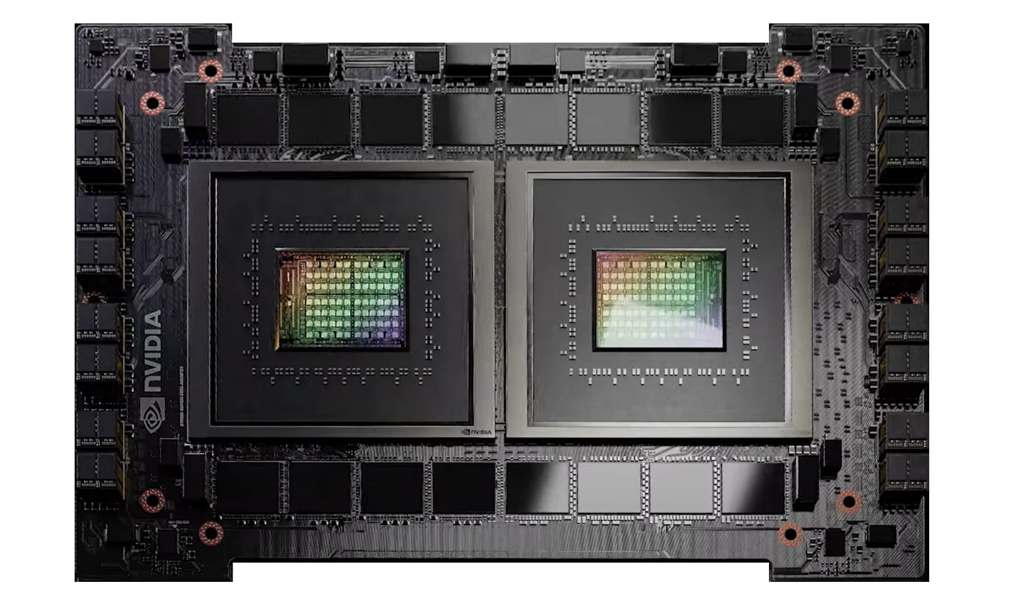
While we only have computer renderings of Grace, we can look at the size and features while we wait for proper photographs of actual Grace silicon. Using the Grace Hopper Superchip and the sizes of power delivery and H100 GPU, the latest renders would indicate a monstrous 700 mm² monolithic die featuring a 12 x 7 mesh grid with 76 cores and 8 memory controllers. Thus, 4 cores would be disabled per die to achieve 144 cores on a Grace CPU Superchip Module. Such a large die also indicates the use of larger ARM cores, most likely an improved generation to the Neoverse-V1 cores used by Amazon’s Graviton3 CPUs. Given the promoted performance numbers and power per unit area of silicon, this indicates a low operational frequency to maximize power efficiency. Consequently, Grace may not be as competitive in raw compute capability to Intel’s future Sapphire Rapids Xeons and AMD’s future Genoa EPYC CPUs, though many memory intensive HPC workloads may favor the bandwidth efficiency of Grace.
Spicing Up Computex
Some have found the new disclosures at Computex to be few and far between, so we hope this article helps add much more flavor to the event. Intel was basically absent from Computex, with no further updates on their Desktop Arc Alchemist discrete graphics cards that are supposed to launch this Quarter. To not leave them out of this publication, we will be presenting our findings on Intel’s most recent event, Vision 2022. While we work on that article, we recommend checking out the brilliant work done by Locuza and SemiAnalysis on their deep-dive on Meteor Lake, a paradigm shift in Intel’s SoC design.
For those who read till the end, here’s a bonus. A new Italian City visited by AMD, famous for the Piazza del Campo. Angstronomics presents the historic Tuscan City of Siena!


In this interview AMD says downlink between CPU to chipset is PCIe 5.0 : https://www.techpowerup.com/review/amd-zen-4-ryzen-7000-technical-details/
Why you say it's PCIe 4.0 ?
Siena? That's Something6 i guess?