Apple A16 Die Analysis
Preliminary Annotation
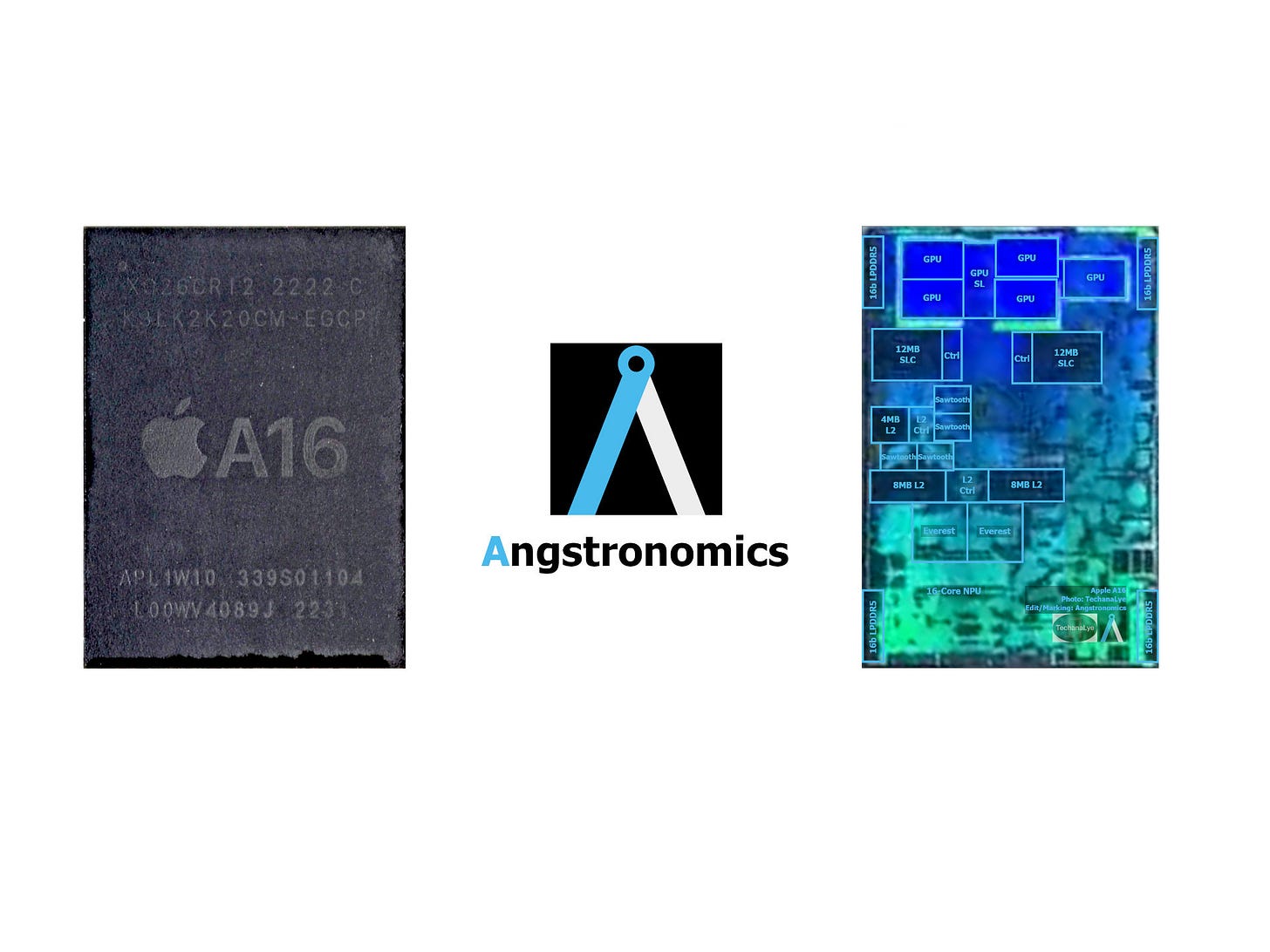
Yoji Shimizu of TechanaLye recently uploaded a teaser video featuring the latest Apple A16 Die. While the resolution is low, there are enough discernible features for Angstronomics to capture frames, compile a Die Shot, and do a simple annotation of the key features on the chip.
Unlike their M-Series Apple Silicon, Apple does not publish die renderings of the A-Series chips for iPhone. As such, we will be making some assumptions based on relative structure sizes to see what we can learn from the first publicly available die shot of the A16.
A16 vs A15
To start, we know that the E-Core Cluster L2 Cache size remains the same at 4MB between both A16 and A15. Therefore, we can get a rough scale of the relative areas if we assume the cache array area is similar between regions as it historically has been.
From this, we can infer that the P-Core Cluster’s L2 Cache has grown from 12MB on the A15 to 16MB on the A16, as the cache array area is about 4x that of the 4MB L2 array. Increasing cache size is an architecturally simple way of increasing energy efficiency by keeping more information closer to the CPU at the expense of more area. This is a 33% jump in cache vs A15, which had a 50% jump vs A14. Clearly there will be diminishing returns as cache scales.
P-Core Cluster L2 Cache
A14: 8MB
A15: 12MB
A16: 16MB
Conversely, it seems the System Level Cache (SLC) has regressed in size, from 32MB on the A15 down to 24MB on the A16 (~6x area of 4MB L2 array). Remember that A15 doubled SLC size from A14, so going back down seems surprising. However, we also note that A16 finally moved to LPDDR5-6400 after 5 years on LPDDR4X-4266 (A11 to A15). This 50% increase in memory bandwidth may be sufficient to offset the smaller SLC capacity.
System Level Cache (SLC)
A14: 16MB
A15: 32MB
A16: 24MB
Layout wise, the format stays mostly the same between generations with the memory, NPU, P-Cores, SLC and GPU all with a similar layout. However, the E-Core cluster has changed positions to be between the P-Cores and SLC instead of beside it.
Area: Slightly Larger
While we cannot accurately determine the area of the A16 chip from the video clip or other sources, we can see that the die size is indeed slightly larger than the A15. We will have to wait for further information to become available to determine the exact area increase. (If one assumes the 4MB L2 array on both A16 and A15 take the same area, that would also give a larger die size for the A16)
Factors supporting this are the 6% increase in transistor count combined with a lower amount of dense cache arrays on die leading to a larger die size to make up that transistor count. This may be enough to offset any transistor density benefits of moving to TSMC N4 vs A15 on N5. It would also make sense that the A16 costs more to produce than the A15, as for the first time ever, the latest chip is only available on the high-end Pro iPhone line, but the primary contributor of cost there would be from more expensive LPDDR5, as the die area differences are not large.
The Everest P-Cores on the A16 appear to be a new core with different internal layout to Avalanche on A15. Area seems similar to marginally larger.
The Sawtooth E-Cores on the A16 also appear to have a different layout from Blizzard on A15, while also taking a bit more area.
The GPU core design on the A16 is not discernible here, but area and performance seem identical to A15.
A16: Asymptote?
Independent testing of the A16 shows that performance improvements have been levelling off, as a direct result of having 3 generations on similar process nodes. Apple can increase die size to get more performance, but that increases costs. As such, A16 is a symptom of Moore’s Law slowing as we continue waiting for the next generation of 3nm-class nodes.


24MB SLC + LPDDR5 seems like a more balanced decision than 32MB SLC + LPDDR4. A15 has the same amount of SLC as M1 Max (108mm2 vs. 420mm2).