The much anticipated RDNA 3 graphics line from AMD has received numerous conflicting and changeable rumors over the past year, from multiple compute dies with hundreds of compute units to wildly different cache and die sizes. It is time for Angstronomics to clear the air, and detail just what RDNA 3 brings.
GFX11: Area, Area, Area
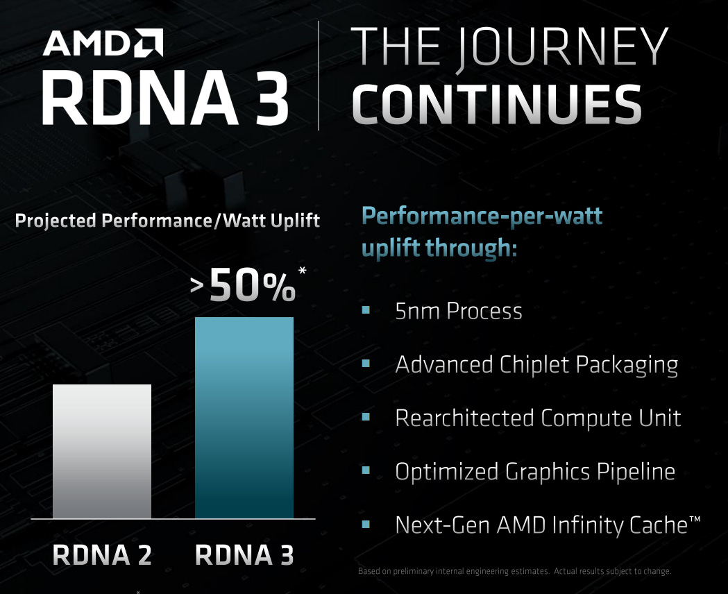
What AMD has officially detailed so far about RDNA 3 is yet another significant increase in performance per watt over RDNA 2, with contributions from process node and microarchitectural design choices. However, the design philosophy of gfx11 is all about area, area, area. What is the best way to achieve the performance target with minimal area? The rearchitected Compute Unit and Optimized Graphics Pipeline changes are mostly about trimming the fat in pursuit of the lowest area and cost (example: halving relative FP64 rate to 1/32). As a result of this focus, PPA is significantly increased. In fact, at the same node, an RDNA 3 WGP is slightly smaller in area than an RDNA 2 WGP, despite packing double the ALUs.
OREO
One of the features in the RDNA 3 graphics pipeline is OREO: Opaque Random Export Order, which is just one of the many area saving techniques. With gfx10, the pixel shaders run out-of-order, where the outputs go into a Re-Order Buffer before moving to the rest of the pipeline in-order. With OREO, the next step (blend) can now receive and execute operations in any order and export to the next stage in-order. Thus, the ROB can be replaced with a much smaller skid buffer, saving area.
Infinity Cache Updates
The Memory Attached Last Level (MALL) Cache blocks are each halved in size, doubling the number of banks for the same cache amount. There are also changes and additions that increase graphics to MALL bandwidth and reduce the penalty of going out to VRAM.
Navi3x dGPU Configurations
Now we will go through the specifications of each die configuration of discrete RDNA 3 GPU. To be abundantly clear, these configurations for Navi3x were done in 2019 and finalized sometime in 2020, with no changes since.
Navi 31
gfx1100 (Plum Bonito)
Chiplet - 1x GCD + 6x MCD (0-hi or 1-hi)
48 WGP (96 legacy CUs, 12288 ALUs)
6 Shader Engines / 12 Shader Arrays
Infinity Cache 96MB (0-hi), 192MB (1-hi)
384-bit GDDR6
GCD on TSMC N5, ~308 mm²
MCD on TSMC N6, ~37.5 mm²
The world’s first chiplet GPU, Navi31 makes use of TSMC’s fanout technology (InFO_oS) to lower costs, surrounding a central 48 WGP Graphics Chiplet Die (GCD) with 6 Memory Chiplet Dies (MCD), each containing 16MB of Infinity Cache and the GDDR6 controllers with 64-bit wide PHYs. The organic fanout layer has a 35-micron bump pitch, the densest available in the industry. There is a 3D stacked MCD also being productized (1-hi) using TSMC’s SoIC. While this doubles the Infinity Cache available, the performance benefit is limited given the cost increase. Thus, the main Navi31 SKU will have 96MB of Infinity Cache (0-hi). This is lower than the 128MB in Navi21. A cut-down SKU will offer 42 WGP and 5x MCD (80MB Cache, 320-bit GDDR6).
The reference card appears to have an updated 3-fan design that is slightly taller than the previous generation, with a distinctive 3 red stripe accent on a section of the heatsink fins near the dual 8-pin connectors.
There were early plans for a version with 288MB of Infinity Cache (2-hi), but this was shelved as the cost-benefit was not worth it.
Navi32
gfx1101 (Wheat Nas)
Chiplet - 1x GCD + 4x MCD (0-hi)
30 WGP (60 legacy CUs, 7680 ALUs)
3 Shader Engines / 6 Shader Arrays
Infinity Cache 64MB (0-hi)
256-bit GDDR6
GCD on TSMC N5, ~200 mm²
MCD on TSMC N6, ~37.5 mm²
Coming in 2023, Navi32 is a smaller version of Navi31, reusing the same MCDs. Navi32 will also be coming to mobile as a high-end GPU offering in AMD Advantage laptops. There were plans for a 128MB (1-hi) version, however it might not be productized due to the aforementioned costs. Thus Navi32’s 64MB is also smaller than Navi22’s 96MB.
Navi33
gfx1102 (Hotpink Bonefish)
Monolithic
16 WGP (32 legacy CUs, 4096 ALUs)
2 Shader Engines / 4 Shader Arrays
Infinity Cache 32MB
128-bit GDDR6
TSMC N6, ~203 mm²
Navi33 is the mobile-first push for AMD. They expect robust sales of AMD Advantage laptops with it, as the design is drop-in compatible with Navi23 PCBs, minimizing OEM board re-spin headaches. They aim to ship more Navi33 silicon for mobile than to desktop AIB cards. The first concepts showed Navi33 as a chiplet design with 18 WGP and 2x MCD, but this could not meet the volume and cost structure of this class of GPU vs a monolithic design.
As an aside, Navi33 outperforms Intel’s top end Alchemist GPU while being less than half the cost to make and pulling less power.
Conclusion
While Angstronomics has disclosed the hard specifications, we did not mention performance and power here. More importantly is how competitive AMD feels their RDNA 3 lineup is compared to market leader Nvidia’s “Ada Lovelace” line of next generation GPUs. We will cover this in a future article, and what AMD is doing about it.


You are so good. These YouTube leakers love inventing stuff and spreading it over 30 minutes, constantly guessing everything. Meanwhile the SKYGOD of Angstronomics is succinctly stating all the details without droning on and on.
No ads, no peddling BS.
Everyone should subscribe to Angstronomics!
Incredible content, no padding, no nonsense or self-aggrandization. Instant subscription from me!