Angstronomics presents the hard truths of the world's most advanced process node. We detail their claims vs real chips, how transistor density is calculated, show concrete measurements on the real dimensions of TSMC N5, and get technical on its transistor layout to explain area scaling. We will follow up with what this means in the context of their next N3 and N2 nodes.
TSMC has remained very tight lipped on technical details about N5. Information for calculating transistor density has not gone far beyond the ‘1.8x vs N7‘ that TSMC said 4 years ago. Their IEDM 2019 paper about N5 was accepted which contained no transistor dimensions. Scotten Jones and David Schor expressed that the paper was more marketing than technical. The paper seemed to have passed muster only because it was about the world’s most advanced process technology.
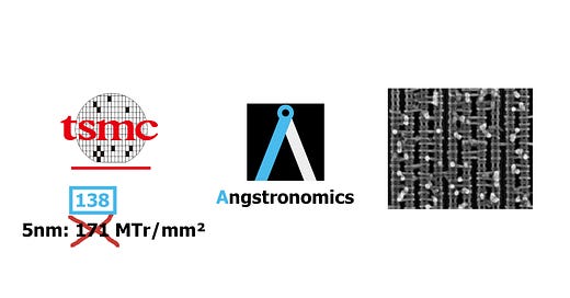
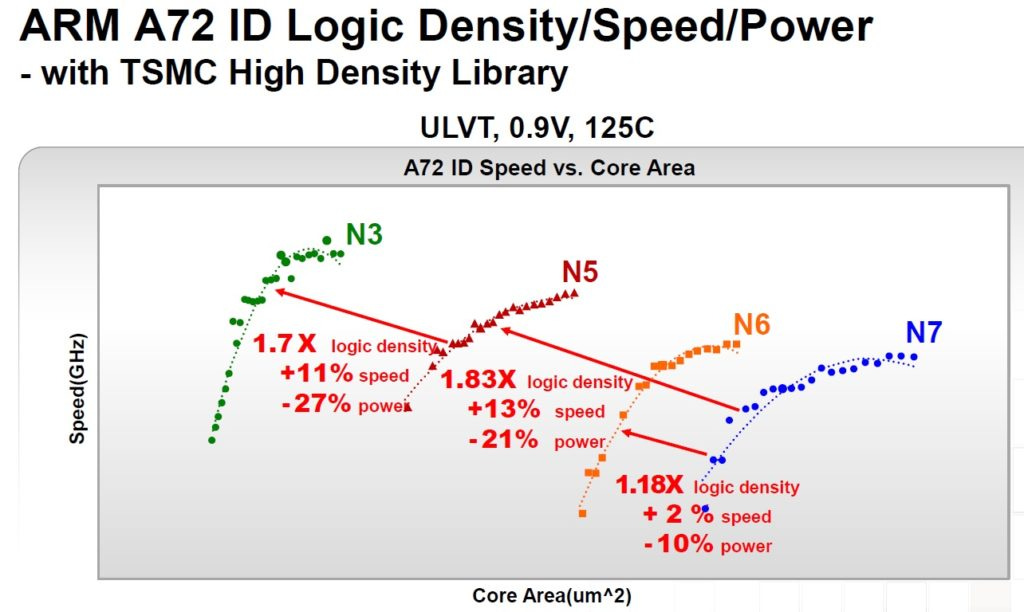
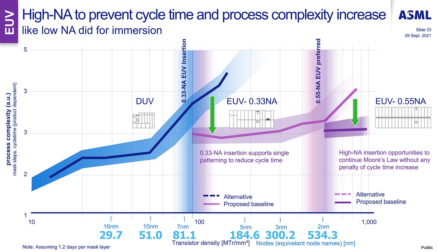
Since then, TSMC’s public disclosures left us with varying 1st party logic density improvement claims, from 1.7x to 1.84x, leading to many incorrect density assumptions from media and even industry. With nothing else to work with, the density claim was simply multiplied with known TSMC 7nm densities to arrive at numbers like 171 Million Transistors per square mm (MTr/mm²). We will explain how transistor density is calculated below. These assumed numbers have been with us for years, even ASML themselves showed just recently that foundry 5nm is over 180 MTr/mm² (relevant slide at the bottom of this article).
But the reality is completely different. The real density is far lower than that. The 1st sign of trouble came almost immediately with Apple’s A14 announcement, the world’s first N5 chip. 11.8 Billion transistors, about 88mm². The average transistor density for the whole chip is 134 MTr/mm². This marked a big divergence in the relation between calculated logic density and average chip density. Mobile AP (Application Processors) have historically just so happened to track closely with theoretical calculated logic density. Something was up. Apple’s design didn't change drastically. Then more and more chips came out. Kirin 9000. M1 Max. None reached the assumed density of 171. The reality is that the correlation still holds. The assumed density is wrong.
MTr/mm² Metric
The theoretical density is calculated using the metric pushed by Mark Bohr of Intel. This metric is used to calculate theoretical transistor density for logic circuits, and is better than previous attempts as it captures area scaling from transistor structure and layout improvements. SRAM and Analog is not used in the calculation nor is the ratio of logic to SRAM to Analog in real chip designs. Officially, the formula is:
To understand how to use this, we must know the important dimensions and structure of logic transistors in modern day circuit design.
Standard Cell Terms and Scaling Vectors
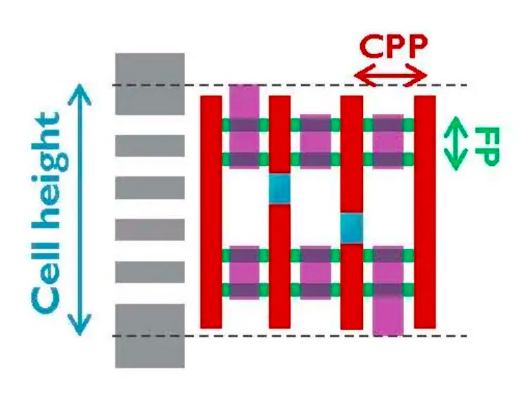
Modern process technology uses Complementary Metal Oxide Semiconductor transistors, mixing PMOS and NMOS to create logic circuits. Standard cells are organized into horizontal rows. Designers build standard logic circuits within these rows like Inverters, NAND gates, adders and flipflop cells that serve Boolean logic functions. The key dimensions to note in transistor area scaling is the Contacted Gate Pitch (CGP, historically poly pitch CPP) in the horizontal x-direction, and Cell Height in the vertical y-direction. This gives the unit cell area which can be used to determine density. Angstronomics will use the following descriptor for node dimensions:
2-fin TSMC N7 (H240g57)
H240 = 240nm Cell Height
g57 = 57nm Contacted Gate Pitch
Logic transistor density scaling comes from reducing these two dimensions. Scaling trends show that the actual transistors themselves (Front End Of Line FEOL) can shrink better than the metal interconnect to wire them (Back End Of Line BEOL). EUV is needed to shrink the lowest metal layers further. CGP is limited by contact width, spacer width, gate length and diffusion breaks. Cell Height is limited by minimum metal pitch, number of metal tracks, and less so fin count and fin pitch. Reducing these dimensions is difficult, and the pace has slowed down considerably. CGP width is barely shrinking at all. Cell height can still scale with Design Technology Co-Optimization (DTCO) techniques such as fin depopulation, Back Side Power Delivery, Complementary FETs (CFET) and others that reduce cell height independent of metal pitch.
Defining the Density Values
With CGP and cell height we can go back to the density calculations. For modern process nodes that have Single Diffusion Breaks (detailed below), a 4-transistor NAND2 cell has a width of 3x CGP. Intel presented 19x CGP for their Scan FlipFlop cell. We will go with that with a 32 transistor circuit inside that area. Angstronomics understands that the CGP width and transistor count of large cells may differ from node to node due to drive current and metal interconnect differences. Nonetheless, 4-in-3 and 32-in-19 is approximate to industry metrics for SDB. Add an additional CGP for each cell for Double Diffusion Break (DDB) nodes such as N7. Inserting these values into the formula, then adding values for Intel’s densest 10nm library (H272g54), we get 100.33 MTr/mm². Intel listed a density of 100.8. For TSMC’s N7 2-fin (H240g57), we get 90.64 MTr/mm². For fun, we can reverse the formula and find pitches that meet the incorrect density assumption for N5. H180g48 would give a density of 170.6 MTr/mm².
Measuring Actual N5 Transistors on Apple A15
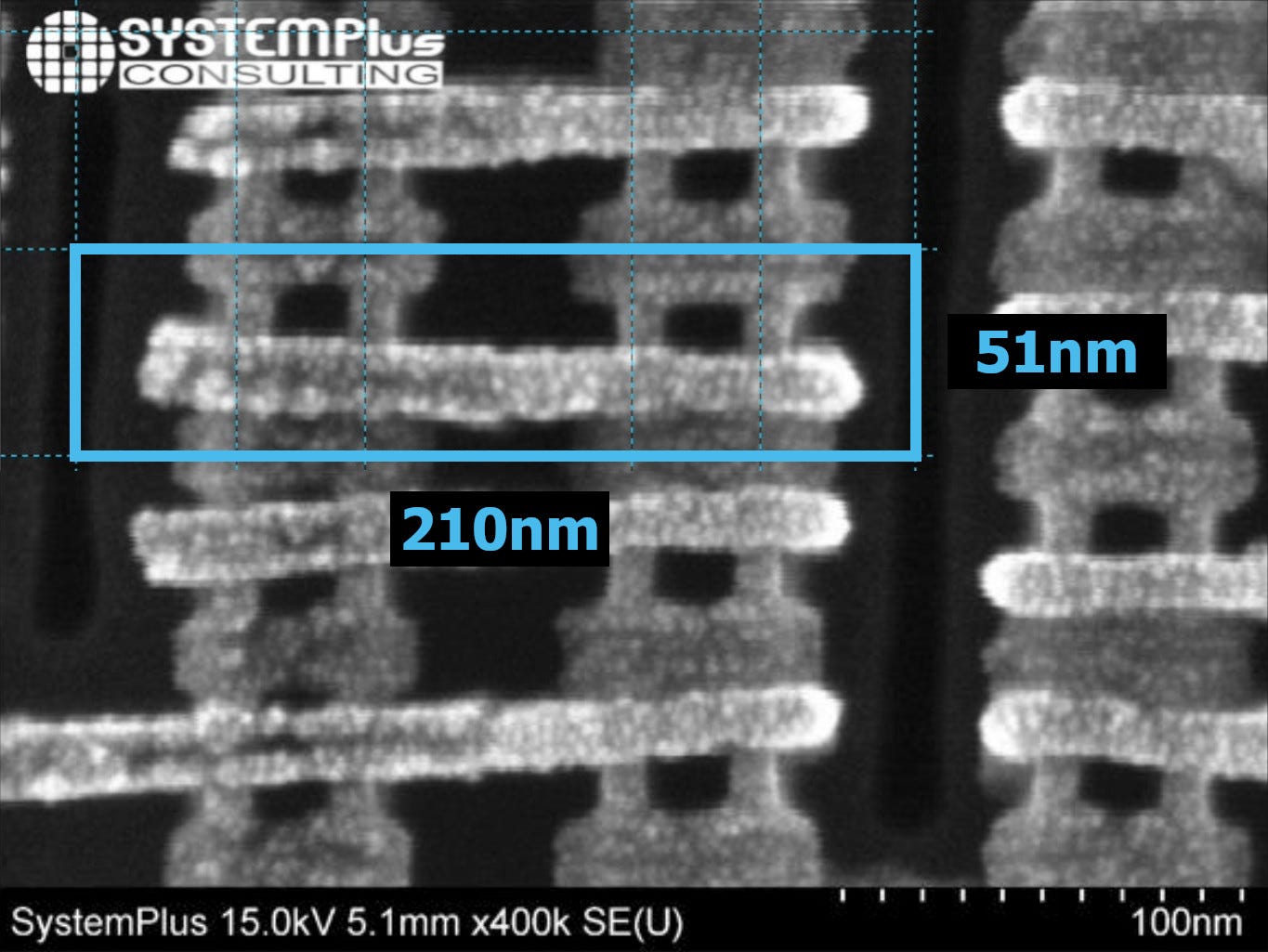
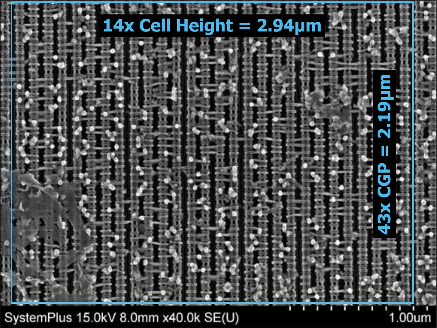
Thanks to System Plus Consulting (now part of Yole Group), we can measure TSMC N5 logic transistors directly. From their Apple A15 Reverse Costing Sample, there are 2 crucial Scanning Electron Microscopy (SEM) images with scale bars that show logic transistors. We measure an average standard cell height of 210nm and average CGP of 51nm. Plugging in those numbers into the density formula shows the H210g51 of TSMC N5 2-fin achieves a logic density of 137.6 MTr/mm². These values match the industry disclosures if one knows where to look [1]. So N5 is 1.518x denser than N7. We also measure a minimum fin pitch of 28nm, which lines up with the 28nm M0 pitch of N5. TSMC disclosed that their N5 has a 30% smaller minimum metal pitch vs their N7 (40nm MMP) [2]. Additionally, a 6-Track cell at 210nm cell height reveals an M2 pitch of 35nm.
Why This Discrepancy?
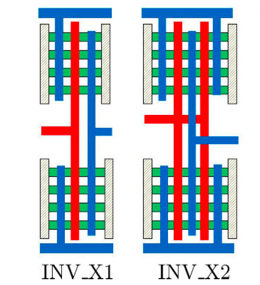
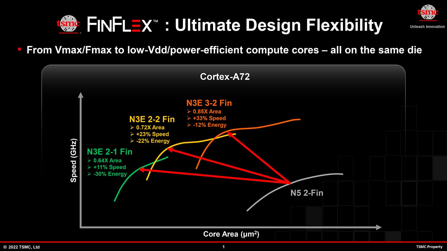
TSMC’s density claims were never based on this density metric or any critical pitch in the first place. They compare using an ARM Cortex-A72 synthesis which is very flexible in layout and area. At a high level, the same core design on the same node and library can trade some area for increased frequency and performance by using larger standard cell variants with higher drive current strengths. An example with the simple logic inverter shows a higher drive strength INV_X2 standard cell can be made with a double-gate design with 2-fingers that takes more area than the standard INV_X1 for the same logical function [3]. This flexibility in design generates a Freq/area curve as presented by TSMC. The foundry can choose to compare any chosen point on one curve with another to derive a density claim ratio.
This kind of comparison is more 'real world' as the node benefits are extracted all the way to a complex CPU core level instead of just blindly estimating density based on raw FEOL pitch as in the Bohr model. As we detailed earlier, scan flipflop and large cells may take up different areas with the same FEOL dimensions based on BEOL aggressiveness which affects signal routing density. Design Rule Check (DRC) push can also provide overall density increase with the same FEOL size at the expense of increased design complexity. One example is reducing the margin width between logic and SRAM regions in silicon. The margin is needed to maintain different silicon strain values for Logic and SRAM to ensure device performance and reliability near region boundaries. Nonetheless, we are still going to call out TSMC here as the average chip density in real processors still lines up with the Bohr model and not their claims.
What Does This Mean for N5?
Nothing. Continue to enjoy your 20-month old iPhone 12 and brand new M2 MacBook. They are wonderful devices. An N5 wafer can still pack close to 10 trillion transistors. N5 has been the world's most advanced node for years. Just not as dense as assumed. Samsung’s 4LPE (H200g54) at 136.5 MTr/mm² is ever so slightly less dense than N5 but arrived 16 months later at vastly lower volumes and low reported yields. Density is only 1 metric in PPA (Power, Performance, Area). Samsung closed the gap in density but performance and power remain behind, with only a small improvement over their 7nm-class node.
What About High Performance Cells?
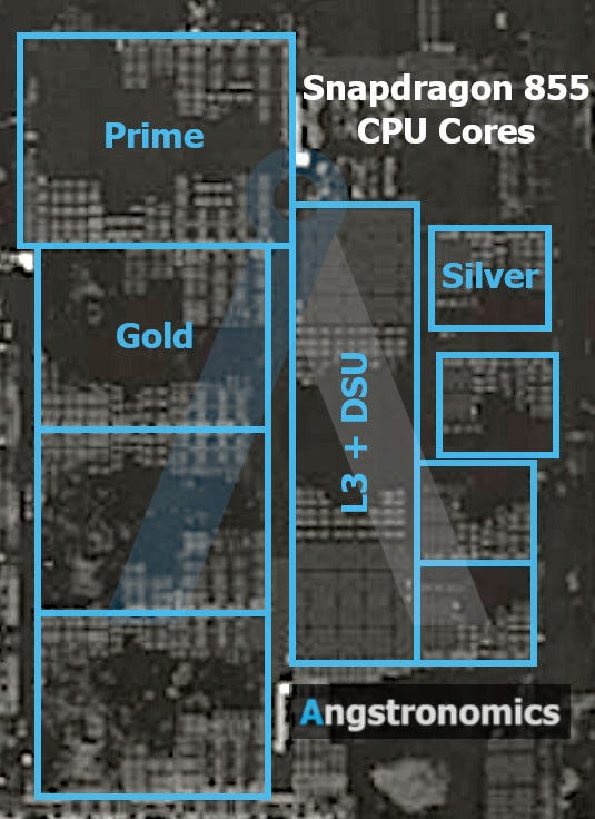
So far we have only featured the densest 2-fin library as it gets all the density plaudits, but High Performance (HP) cells are also important for high performance computing and low latency serial applications. We saw with Qualcomm’s Snapdragon 855 on TSMC N7 use selective 3-fin HP (H300g64) cell region for a Prime CPU core over the standard 2-fin library (H240g57) to get more single thread perf at the expense of some area. Adding 2 more fins to the dense cell to get 3 PMOS + 3 NMOS fins, and adding 1 more Metal-2 track and relaxing pitches, we get a cell height of 280nm (7-Track 40nm M2). For CGP, the value is 57nm, which is the same as 2-fin N7. This tracks historically with TSMC’s HP cell using the same CGP as their previous generation HD cell (N7 HP = N10 HD = 64nm CGP). H280g57 gives a logic density of 92.3 MTr/mm² for 3-fin N5. Coincidentally, this just happens to be around the average chip density of NVIDIA’s H100 and Alibaba Yitian 710.
Now we observe that 3-fin N5 has a lower density than the 3-fin Intel 4 process. Intel 4’s sole 3-fin library (H240g50) has a density of 122.8 MTr/mm². Of course, Intel 4 products come years after N5 at much lower wafer volumes. Intel 4 is also an incomplete node, only offering a single 3-fin library and a minimal I/O library for chiplet-only interconnect to accelerate Time-To-Market (TTM). However, Intel 4 has a significant DTCO advantage over N5, as it achieves much higher density despite using a wider metal pitch and fewer EUV layers. They achieved aggressive cell height reduction by narrowing the space between n and p diffusion regions with a much narrower gate cut width. This significantly increased the percentage of active fins to patterned fins. We also expect Intel 4 to have better Performance/Power due to better metal interconnect material composition of Cobalt-wrapped Copper.
CNOD and Low Vertical Scaling
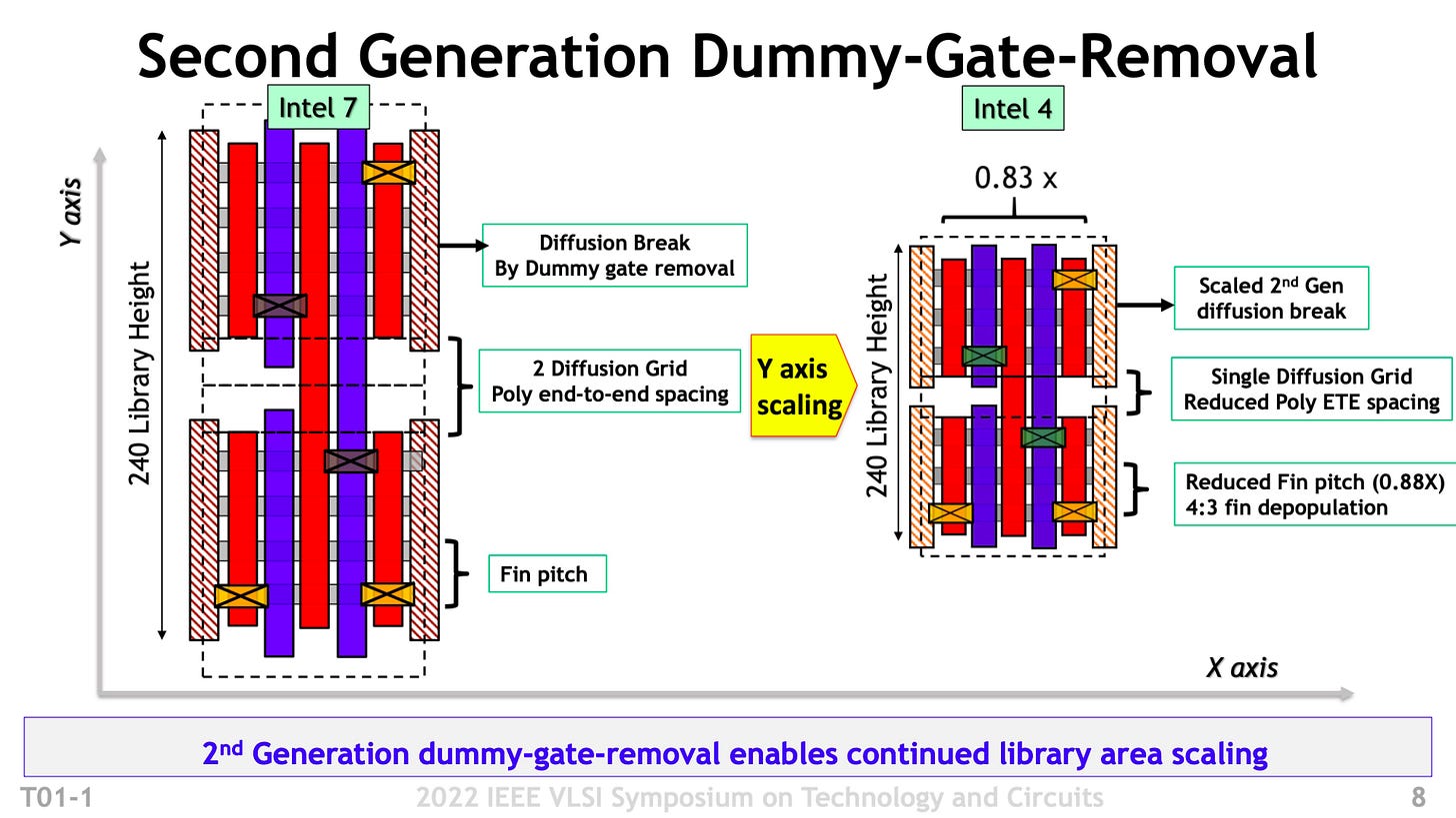
Readers with a keen eye will notice that cell heights have barely reduced going from N7 to N5. 300nm to 280nm for 3-fin and 240nm to 210nm for 2-fin. This is despite the vertical critical dimension (M0) reducing drastically from 40nm to 28nm. One of the reasons is that N5 2-fin now has 5 M0 signal lines between power rails vs 4 M0 signal lines on N7 2-fin. This allows for greater flexibility in contact placement. The other reason is that N5 uses an uncommon form of horizontal standard cell separation called Continuous Diffusion (CNOD).
To separate horizontally adjacent standard cells in the same row, dummy gates are used at the sides of each standard cell to separate one active diffusion area from another. In Double Diffusion Break (DDB), two dummy gates cut-off and separate the active areas. In Single Diffusion Break (SDB), space for a single separation gate is replaced by a deep etched insulator material which cuts the fins and isolates the active areas. This takes up less horizontal width than DDB, contributing to DTCO area scaling.
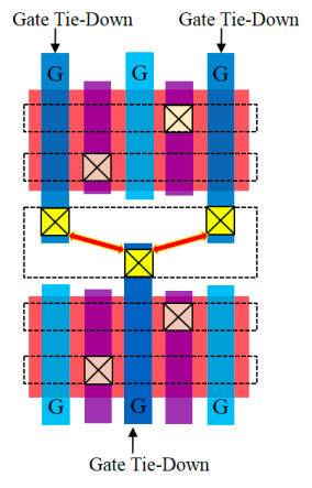
In CNOD, the diffusion is not broken at all. The fabrication process continues normally, but when standard cells need to be separated, the gate between them is designated as a dummy gate. This dummy gate is then connected to a Gate Tie-Down Via to the power rail. This dummy gate tie-down method of CNOD achieves the same horizontal width savings as SDB, and has the advantage of keeping the transistor diffusion unbroken and thus can achieve more uniform strain and performance characteristics. As a refresher, since 90nm, transistors have been made such that the channel where electrons flow is stretched or squeezed under great force which increases channel mobility in order to reduce resistance. SDB relies on the etched insulator region to maintain the physical strain which can have more variability.
The problem with CNOD is the need to tie-down the dummy gate to the power rails. This adds more Vias and connections in the critical region under the power rail, which is between vertically adjacent cell rows. This means the cell height has to increase to accommodate the space for additional contacts between standard cells. While EUV and self-aligned gate contacts do help, CNOD ultimately sacrifices some y-scaling to achieve x-scaling. CNOD is therefore uncommon as the overall area scaling is worse than SDB. SDB can also achieve better isolation as the active diffusions are physically broken and separated. SDB is the standard moving forward, and TSMC uses it in their later N6 and N3 offerings, known as CPODE (Common Poly on Diffusion Edge).
So Can We Trust Their Claims on N3E?
TSMC recently put out their N3E FINFLEX™ figures, once again in their A72 Freq Vs area plot. The rough guide given for combined area scaling contribution was 50% logic 30% SRAM 20% Analog. Logic would have to pull the weight as SRAM and Analog fundamentally cannot benefit from DTCO area scaling. In this case however, A72 core area scaling is much more inline with logic area scaling, giving us a result of 215 MTr/mm² for the densest N3E 2-1 Fin library. Angstronomics already has most of the critical dimensions for TSMC's 3nm offerings, and we will detail them when we can properly cover the debacle that is N3 and the walk back with N3E. As you can see, the actual logic densities are far lower than the 300 Million transistors per sq. mm that some investor presentations have shown for a foundry 3nm process.
The defining technology of TSMC’s 3nm libraries is FinFlex. Angstronomics sees that FinFlex seems to be misunderstood by some. It is not simply selective region cell rows as seen on the Snapdragon 855. Nor is it different ratios of PMOS to NMOS fins (FinFET physics allow the beta ratio to be closer to 1:1). TSMC’s FinFlex video illustrates the actual structure of the standard cell layout. N3 has a 3 fin cell row, 2 fin cell row and 1 fin cell row. That means each standard cell row will have 3 PMOS fins and 3 NMOS fins, 2P+2N fins or 1P+1N fin between power rails. The difference with FinFlex is the hybrid cell row structure.
3-2 fin means alternating rows of 3p3n and 2p2n. 2-1 fin means alternating rows of 2p2n and 1p1n. This alternating cell row layout provides more cell library density options before the move to nanosheets where library density no longer has to be quantized by fin count (although in reality the metal stack and cell rows provide some level of discrete units). Of course, this unique hybrid row layout means a complete rethink of standard cell designs. Engineers have to think about which transistors in a logic block to put in each alternating low and high fin count cell rows based on device performance characteristics. Design Rule Complexity gets even more complicated. Electronic Design Automation (EDA) software has to take the hybrid rows into account.
Single-Fin Library (N3S?)
TSMC VP Kevin Zhang mentioned the existence of another 3nm variant called N3S, arriving later in 2024+ and is said to be a transistor density optimized process. Historically, process variants do not normally change fundamental critical dimensions outside of a small relaxation in CGP to enhance yield and performance. Thus, Angstronomics believes N3S may offer a Single-Fin Only Library to squeeze out the last drop of transistor density.
Though an ultra-dense single fin library might grab headlines with its transistor density, there is a big catch. The practicality of such a library is subject to scaling bottlenecks by the metal stack. Each transistor still has to have its Gate, Source and Drain terminals connect to the metal interconnect network to function. Despite the best efforts of current EUV lithography, the lowest metal layers form the largest bottleneck in lowering cell height and reducing area. There is no point making the FEOL very small if your BEOL cannot keep up. If you shrink the metal stack through brute force, the wires and spacing become too thin to maintain good resistance and capacitance characteristics. An exclusive 1-fin library would thus not meet the performance requirements for many designs. Although N3S might bring that single fin only library, we believe it may be of limited use due to the sacrifices in transistor performance. Nonetheless, if the density benefits are worth it, designers will find a way to work around these constraints.
TSMC N2: >1.1x Chip Density
As for N2, our preliminary findings show a conservative 1st attempt at nanosheets, with low density improvements, instead targeting better power and performance by moving to Nanosheet transistors. Area scaling grinds to a crawl! Additional risk factors such as Back Side Power Delivery Network will be implemented carefully over the life of N2's derivatives and successors. This reminds us of TSMC’s FinFET transition with their 16FF process, that also had a low density improvement over planar. In addition, while the first devices on N2 are for 2026 onwards, the node can fall back on multi patterning low-NA EUV. Depending on industry execution, risk management may see High-NA introduction on N2 akin to N7+ dipping their toes into the EUV pool. High-NA is not a magic bullet and comes with many challenges from the anamorphic magnification such as directionality, extreme narrow depth of field for photoresists to work within, and alignment and integration with existing full-field processes used on everything but the critical layers.
TSMC N5 is Not as Dense as You Think
So that's it. The cat is out of the bag. You now have the true density of the world’s most advanced process node. The next time you see transistor density numbers from research and tool vendor roadmaps, just remember to dial those back by several notches. Angstronomics will cover the effect of slowing transistor area scaling on the long-term health of Moore’s Law in the Angstrom Era once we detail offerings from the other two remaining leading edge Logic foundries: Samsung and Intel.
References
[1] A. Nayak et al., "A 5nm 3.4GHz Tri-Gear ARMv9 CPU Subsystem in a Fully Integrated 5G Flagship Mobile SoC," 2022 IEEE International Solid- State Circuits Conference (ISSCC), 2022, pp. 50-52, doi: 10.1109/ISSCC42614.2022.9731604.
[2] J. C. Liu et al., "A Reliability Enhanced 5nm CMOS Technology Featuring 5th Generation FinFET with Fully-Developed EUV and High Mobility Channel for Mobile SoC and High Performance Computing Application," 2020 IEEE International Electron Devices Meeting (IEDM), 2020, pp. 9.2.1-9.2.4, doi: 10.1109/IEDM13553.2020.9372009.
[3] S. K. Marella, A. R. Trivedi, S. Mukhopadhyay and S. S. Sapatnekar, "Optimization of FinFET-based circuits using a dual gate pitch technique," 2015 IEEE/ACM International Conference on Computer-Aided Design (ICCAD), 2015, pp. 758-763, doi: 10.1109/ICCAD.2015.7372646.
[4] S. Badel et al., "Chip Variability Mitigation through Continuous Diffusion Enabled by EUV and Self-Aligned Gate Contact," 2018 14th IEEE International Conference on Solid-State and Integrated Circuit Technology (ICSICT), 2018, Fig.2,9, doi: 10.1109/ICSICT.2018.8565694.








3D binary and 3D transistor/resistor 3D binary square 4 and triangle 3 goes into every number except 1 2 and 5 at the beginning of a binary ....which is common some numbers have more than one combination triangles and squares make every 3D shape even a sphere example 10 = 1 square and 2 triangles which makes a pyramid and x amount of pyramids makes a sphere 3D shapes can carry anything ...software frequencies video energy
3D transistor/resistor the space between two number like 1 and 2 is 1 and quarter 1 and half exc but the space between two number that are the same is big and fast.....example 10 ................................2x5=10pulse10=5x2..........................................................................same number different addresses if u use the formula with 3D shapes it can carry anything ...if u make a transistor with all the possible shapes using numbers....it can correspond with the same numbers with the times table numbers and go thro the space/pulse
#3barbaraschrepel